Introduction
Atomically thin transistors are emerging as a promising technology for the future of computing. These transistors, each only about three atoms in thickness, can be stacked to create denser integrations and more powerful chips.
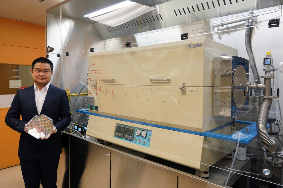
MIT researchers have demonstrated a novel technology that can effectively and efficiently “grow” layers of ultrathin 2D transition metal dichalcogenide (TMD) materials directly on top of fully fabricated silicon chips.
What are Transistors
Transistors are the fundamental building blocks of modern electronic devices. They act as switches, controlling the flow of electrons in circuits to perform a wide range of functions. They are made up of a semiconductor material, usually silicon, with three layers – the emitter, the base, and the collector. By applying a small voltage to the base, the transistor can amplify and switch electronic signals.
Traditional transistor technology
While traditional transistor technology has powered the rapid advancement of electronics over the last few decades, it has its limitations. One major issue is the physical size of transistors, which have been shrinking steadily but are now approaching their limits.
Additionally, as the demand for more computing power increases, the need for denser integrations of transistors becomes more important. Traditional transistor technology struggles to achieve these dense integrations due to the challenges of manufacturing and scaling.
Traditional transistor technology’s limitations necessitated new innovations, such as the development of atomically thin transistors to overcome those challenges.
MIT’s breakthrough in atomic transistors
MIT scientists have made a breakthrough in the development of atomically thin transistors for computer chips. They have effectively grown layers of 2D transition metal dichalcogenide materials directly on top of fully fabricated silicon chips, enabling denser integrations.
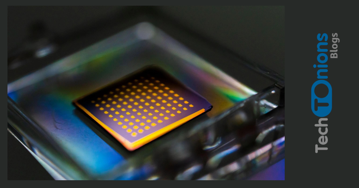
By using molybdenum disulfide, the researchers were able to create ultrathin transistors, each only about three atoms thick, which can be stacked to create more powerful chips. The novel technology they used for the layer-by-layer growth of this transistor makes it possible to optimize its performance.
The issue is that semiconductor chips are generally manufactured using bulk materials. These are somewhat ‘bulky’ 3D buildings. As a result, stacking numerous layers of transistors to achieve denser integration is extremely challenging. But what if two-dimensional designs were possible?
The process of growing thin layers of molybdenum disulfide on a surface is known as metal-organic chemical vapor deposition (MOCVD). Molybdenum hexacarbonyl and diethylene sulfur compounds evaporate, decompose into smaller molecules, and heat up inside the reaction chamber to produce atomically thin transistors.
Benefits of atomically thin transistors
Atomically thin transistors offer several benefits over traditional transistor technology, primarily by enabling denser integrations of transistors on computer chips. Traditional transistor technology approaching its limits, atomically thin transistors made from ultrathin 2D materials offer a solution to continue improving computing power.
By stacking these transistors, the density of transistors on a chip can increase significantly, leading to faster and more efficient computing. Additionally, atomically thin transistors offer new possibilities for types of computing devices that were previously impossible with traditional transistor technology.
Conclusion
In conclusion, the development of atomically thin transistors by MIT scientists represents a significant breakthrough in the field of electronics.
The technology used by MIT to “grow” layers of 2D materials on top of fully fabricated silicon chips is particularly impressive. It allows for precise control over the material’s properties, optimizing its electronic performance.
Overall, MIT’s research on transistors is a significant step forward in the development of new transistor technologies and represents an exciting avenue for the future of electronics.