Table Of Contents :
- AND Gate Symbols
- AND Gate Truth Table
- AND Gate IC’s
- Basic AND operation using 74HC08 IC
- AND Gate Using Transistor
- AND Gate Using Diodes
- Application Of Digital Logic AND Gate
- Conclusion
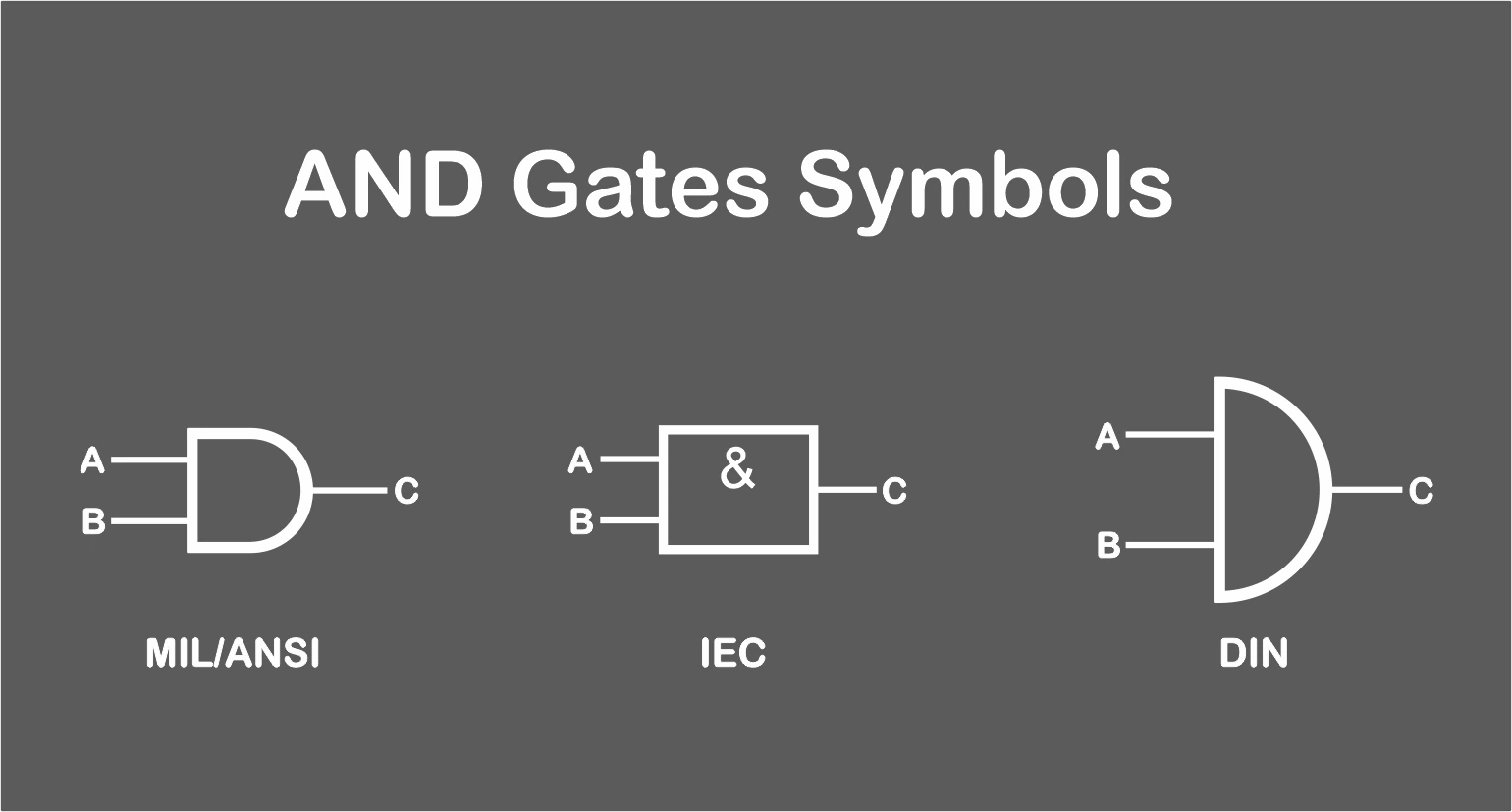
AND Gate Symbols
Let’s start with the AND gate symbols. The most widely used AND gate symbol is from the ANSI symbol, and we will use this for our tutorial. Another AND gate symbol is from IEC symbols. And the last symbol we see is from DIN symbols.
AND Gate Truth Table
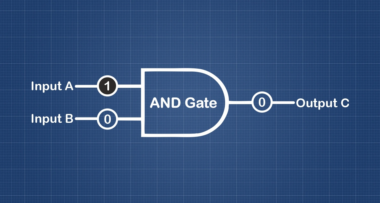
Here is the AND gate truth table, and as we see, the digital logic AND gate only give an output HIGH or logic 1 when all inputs of AND gate are HIGH or logic 1.
If any of the input will be LOW or logic 0, the digital logic AND gate output will also be LOW or logic 0.

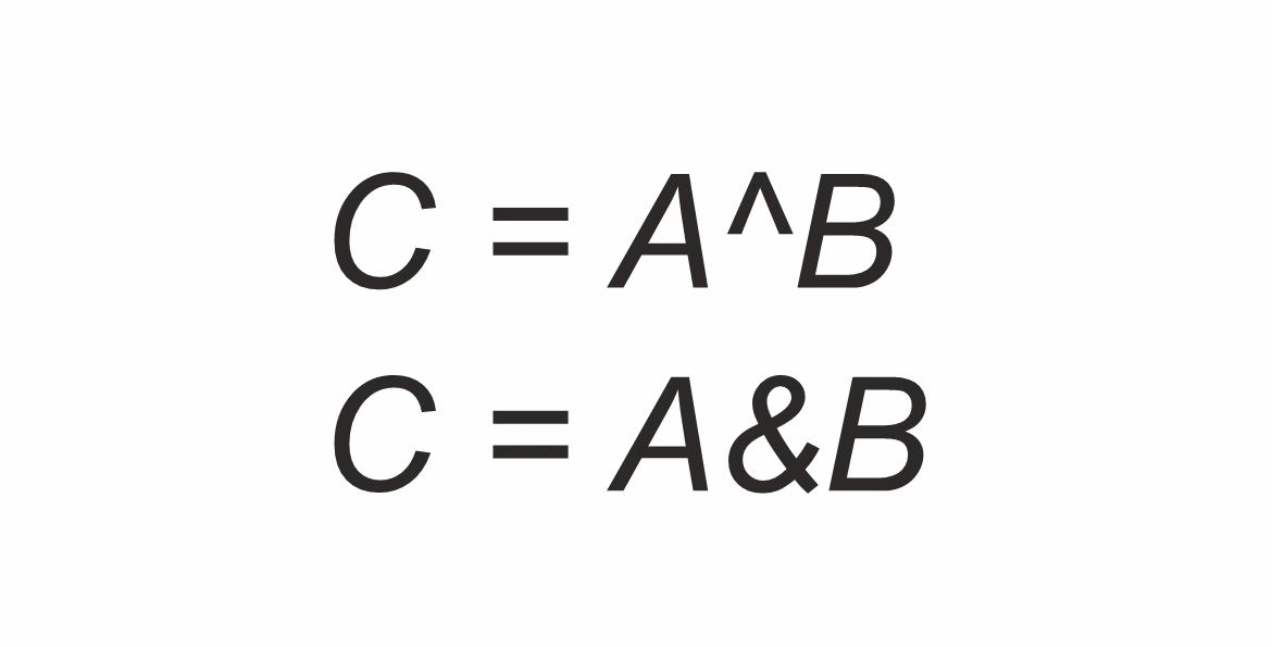
Due to this digital logic AND gate property, the logical expression for the output state is given by logical multiplication denoted by dot (.).
Therefore for an AND gate output as C and having inputs A and B, the equation for output C is.

All inputs are multiplied means any input will be 0; the result after multiplying will be 0, output C will be 0. The output equation is also written as.
Hence digital logic AND gate output will be TRUE if all its input is TRUE. AND gate is also known as the coincidence gate due to this property.
AND Gate IC’s
Many AND gate IC’s are widely used, and they are mainly categorized into two categories. First, it is categorized as TTL-based and CMOS-based.
And further, it is classified based on the number of Inputs that AND gate has.
TTL based
TTL stands for Transistor-Transistor Logic, and it is the earlier transistor-based technology in which transistor is used inside to perform AND logic operation.
Common TTL based AND gate IC’s
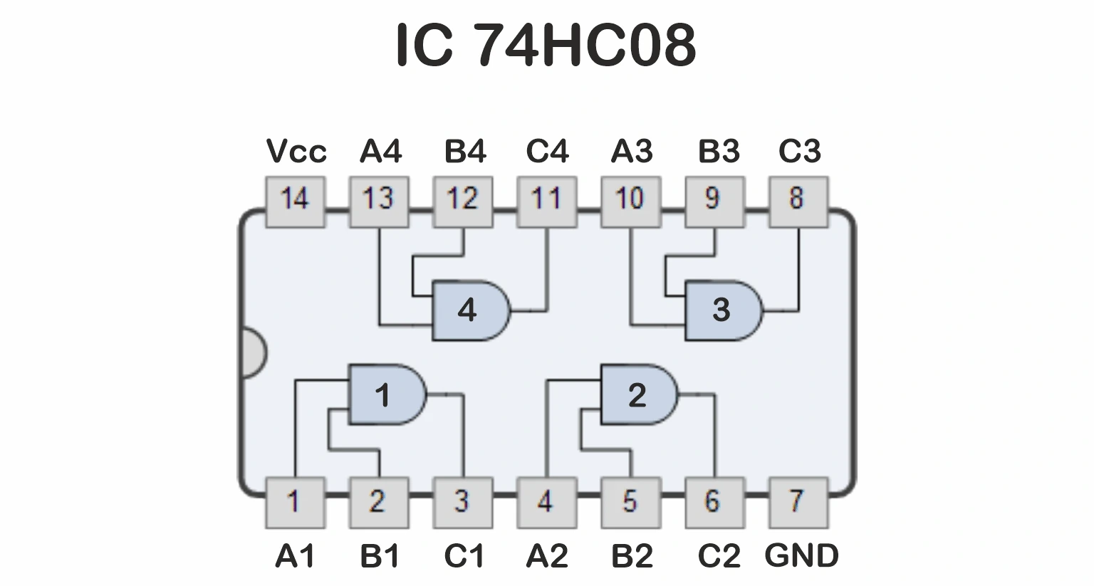
- 74HC08 Quad (2 input AND gate)
- 74HC11 Triple (3 input AND gate)
- 74HC21 Dual (4 input AND gate)
CMOS based
CMOS stands for complementary metal-oxide-semiconductor. It is the latest technology that uses MOSFET for performing AND logic operations. CMOS-based IC is very power efficient as compare to TTL-based.
Common CMOS based AND gate IC’s
- CD4081 Quad (2 input AND gate)
- CD4073 Triple (3 input AND gate)
- CD4082 Dual (4 input AND gate)
Basic AND operation using 74HC08 IC
We will explore 74HC08 Quad AND logic gate IC for this tutorial. We will simulate a simple circuit based on this IC to justify the AND gate operation.
Before starting few things to know about 74HC08 IC
- Its recommended supply voltage is between 2v to 6v.
- It has 4 AND gates with two inputs each.
- Max continuous output current +-25mA.
By considering the datasheet, we will use a 3.3v button cell as an input for this example. You can use a voltage level between 2v to 6v.
Note:- Don’t use 9v batteries. It can fry 74HC08 IC.
Here is the circuit diagram that we will use to demonstrate the usage of 74HC08 IC.
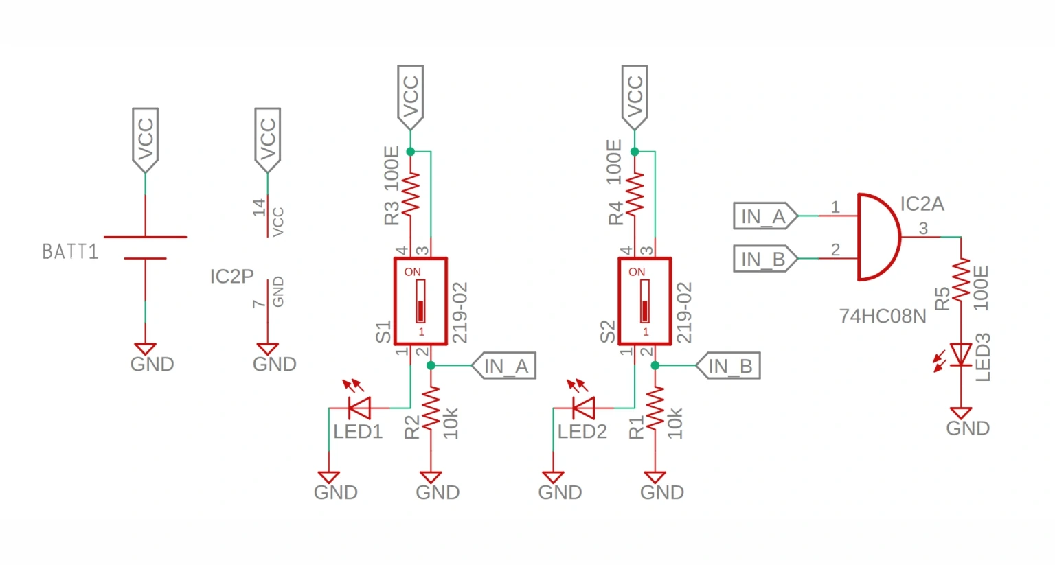
We will use 1 AND gate inside this IC. We will connect both input pins 1 and 2 with pull-down resistors. Therefore ideally, both inputs will be at logic level 0.
We will add two switches to each input pin and another switch pin to the VCC pin to change the logic to 1.
Additionally, we have added LED to each switch so that LED will glow when logic 1 is given to the input pin of the digital logic AND gate.
PIN 3 is the output of the first AND gate. We will connect that to an LED with a current limiting resistor.
Check out more on Current limiting resistors for LED.
Inputs are named as input A and input B. Output is named as Output C.
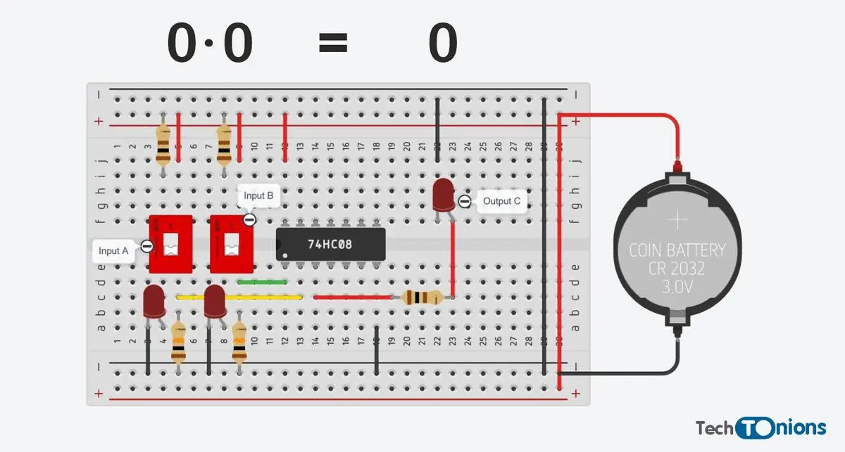
Therefore the output LED will only glow when both the input is HIGH, or 1 and both inputs LED are glowing.
We can compare now the truth table of AND gate with the following simulation outcome.
To Simulate above code click open simulator button given below
AND Gate Using Transistor
Let’s dig deeper, exploring the working of an AND gate using a Transistor model. We can build the exact functioning circuit of AND gate using transistor also.
The number of transistors will require equal to the number of inputs of AND gate required.
All transistors are connected in series with the load (in our case, it’s an LED). So that when both Transistors are in conducting state, then only our load will conduct current means LED will be ON.

We will build a two-input generic AND gate; therefore, we will require two transistors. We have used 2 NPN transistors.
We will provide logic inputs to the transistor base; therefore, if any input is LOW, then the particular transistor will not conduct, and it is connected in series. Therefore, the output will also LOW.
Hence it will follow the same truth table as digital logic AND gate have.
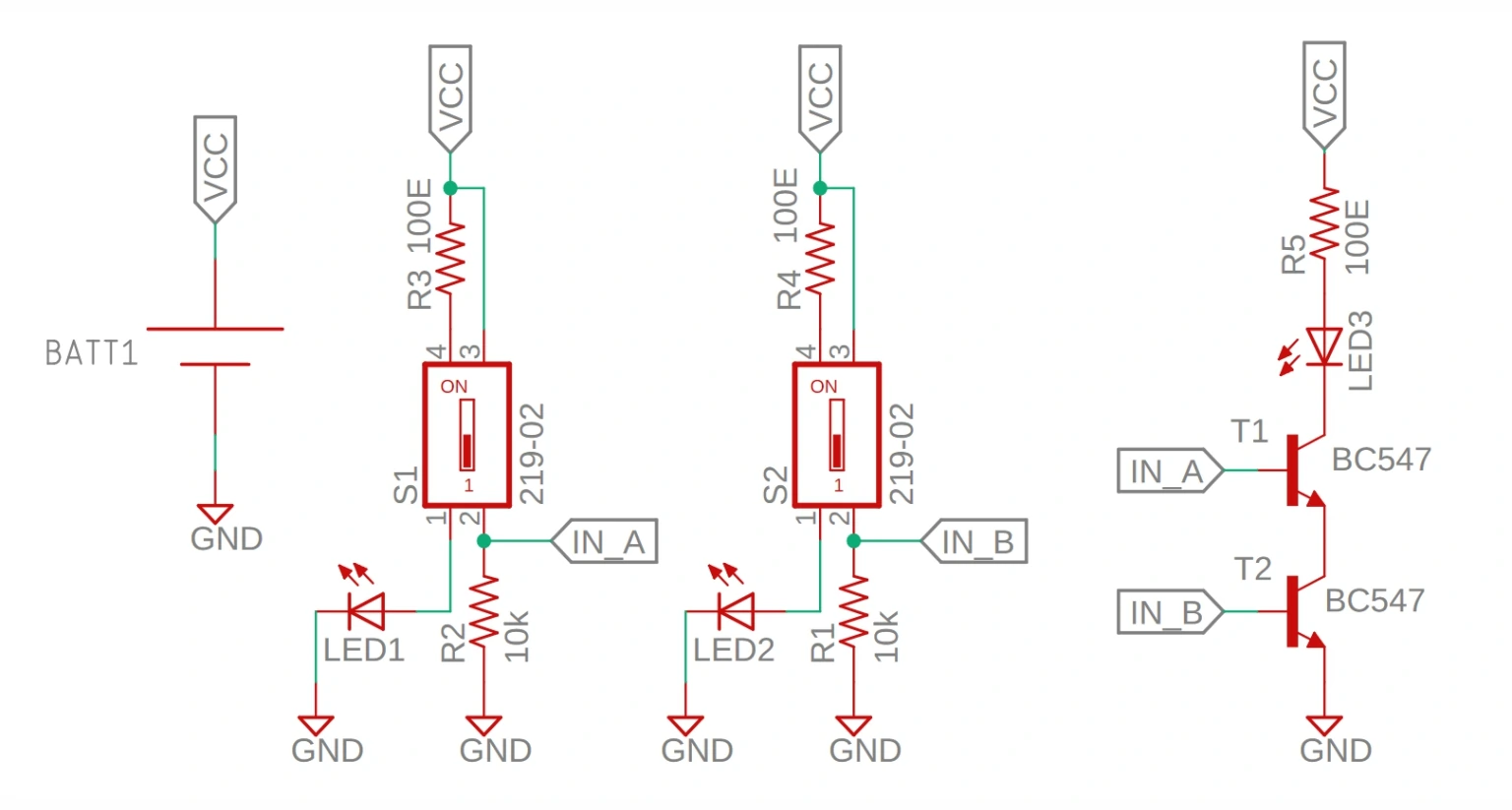
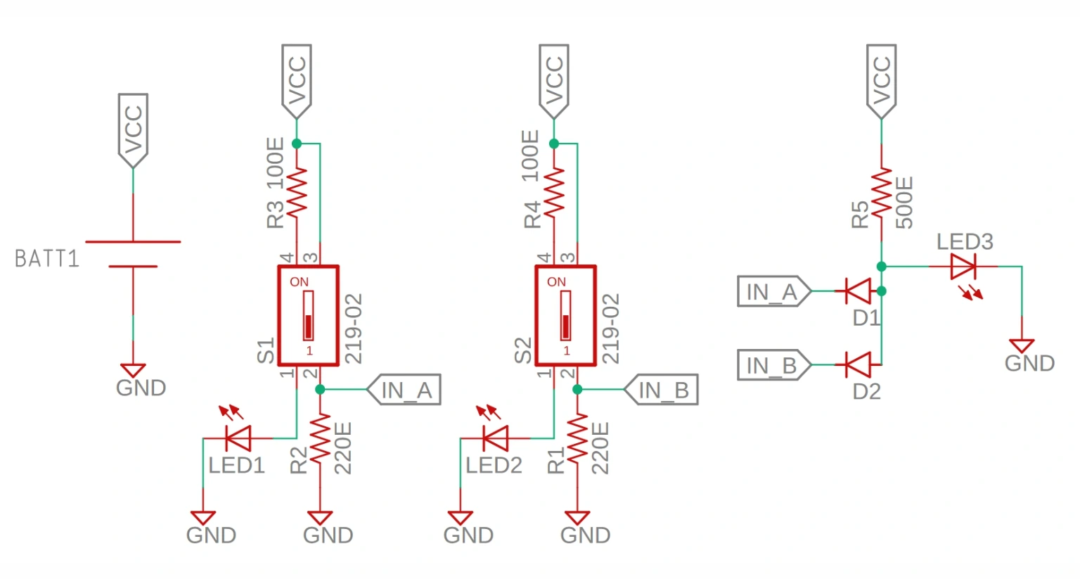
Like the 74HC08 simulation, we will connect input A and input B with a pull-down resistor and a switch connected with VCC to change the input logic level. Additionally, LEDs are added for visual indication of the logic level at the input and output side.
When both input switches are at the ON position, only the output LED is ON. Both inputs LED also ON, indicating that all inputs are HIGH.
If any switch is at the OFF position, the output LED will not glow. Therefore it satisfies the AND gate truth table.
To Simulate above code click open simulator button given below
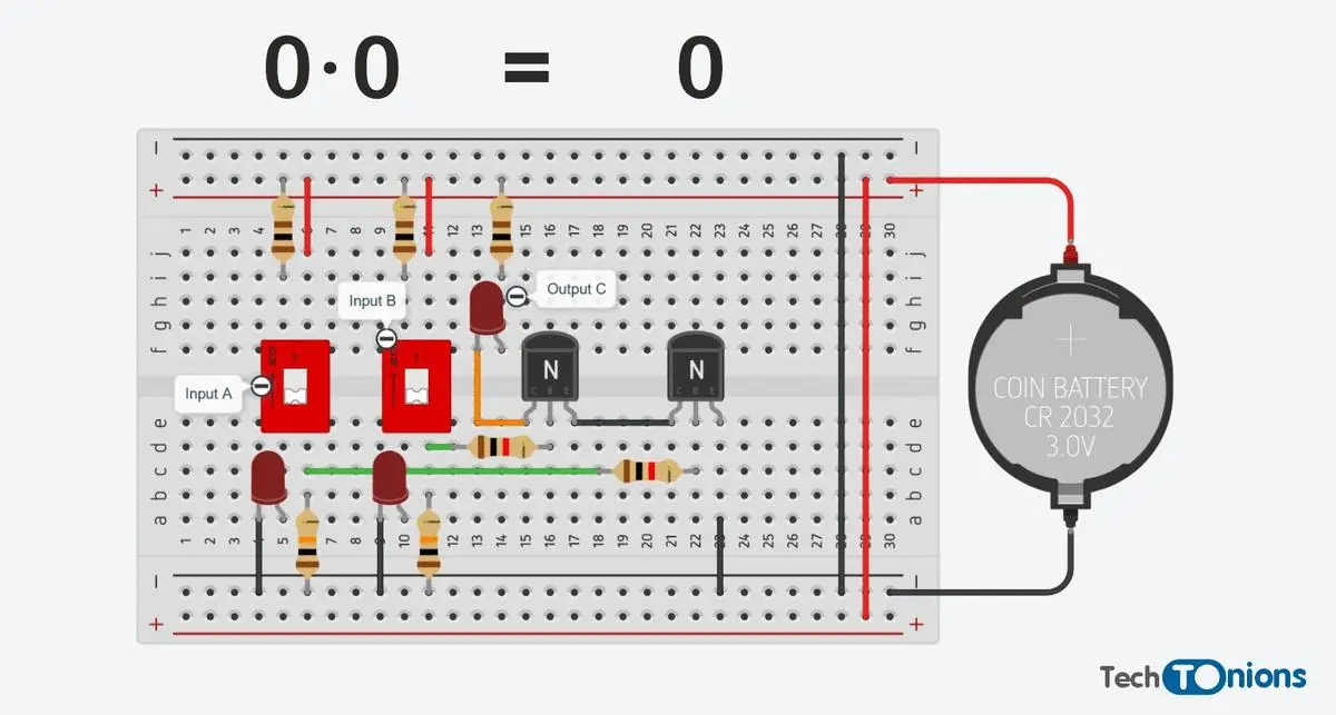
AND Gate Using Diodes
We can also use diodes to build a digital AND gate logic. The numbers of diodes required to do are also the same as the number of AND gate inputs required.
We will build a two-input AND gate by using two diodes in our circuit. The cathode of each diode will work as an input of AND gate.
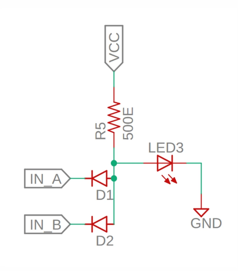
This circuit also has a similar input switch with pull-down resistors and another end to VCC to change the input logic level.
The Anode of all Diodes is connected with a resistor connected to VCC.
Therefore if any cathode of diodes has a logic level low(connected to ground), the current will pass through the resistor and then ground through the diode. As a result, our output LED will not turn ON.
And if both input (cathode) of the diode is connected to HIGH (VCC), the current will not pass through diodes as there is no potential difference across the diode. Hence current will pass through the output LED, and it will glow now.
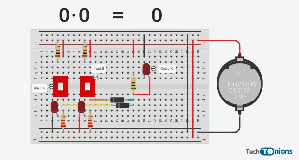
As a result, we can see that only the output LED will be ON when both the switch are at the ON position. As we see the circuit will satisfy the AND gate truth table.
To Simulate above code click open simulator button given below
Application Of Digital Logic AND Gate
AND gate can be used in many projects or integrate to achieve specific tasks. We have come up with a similar real-life application based on AND gate.
In this example, we will build a simple circuit based on 74HC08. You can use any similar AND gate IC.
The application of the circuit will be to monitor the light intensity, and there will be one switch. The output pin of IC drives the small bulb.
If the light intensity is more, it means its day time; therefore, the switch should not work because we don’t need light. And the same switch should turn ON and OFF the light bulb when there is low light intensity (nighttime).
“Stop the light bulb to be turning on in Day time using AND logic“
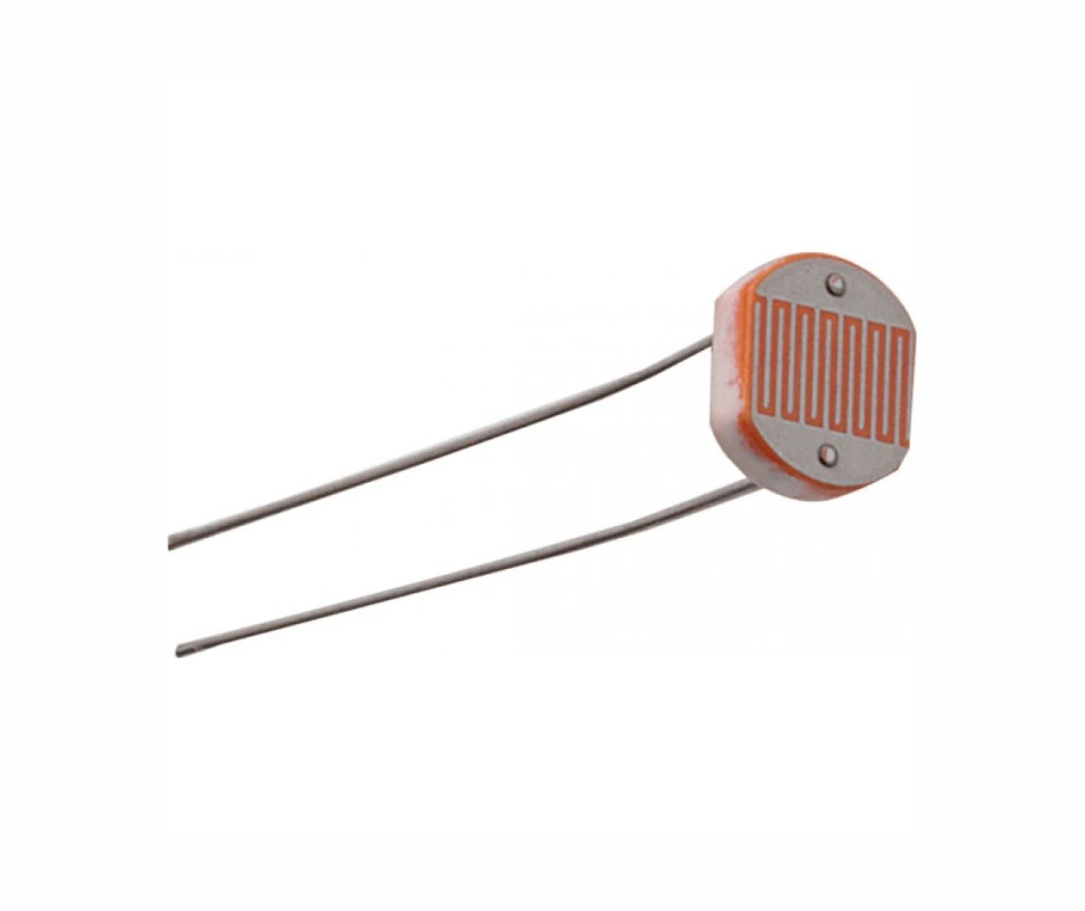
We will use an LDR known as Light Dependent Resistor. It’s a resistor that changes its resistance based on light falls on it. When there is more light intensity, its resistance is low and acts as a close circuit. And when there is low light intensity, its resistance will increase, and it will behave as an open circuit.
Therefore we will connect a combination of pull-up resistor and LDR to one of the inputs of AND gate. Hence this combination will make sure that in the daytime, this input will always be at a LOW level as current will pass to ground through LDR due to less resistance.

And in the nighttime, the LDR will act as an open circuit; hence it will give HIGH input signal to the AND gate.
Now on another input pin of AND gate, we have added a simple switch with a pull-down resistor and one end connected to VCC. Such that it will give HIGH logic input when turned ON and LOW logic input when turned OFF
The output pin is connected to an NPN transistor to drive the load (bulb) as the IC’s output cannot drive a high current. Instead of using a transistor, you can also use a relay module to control an AC appliance with a relay.
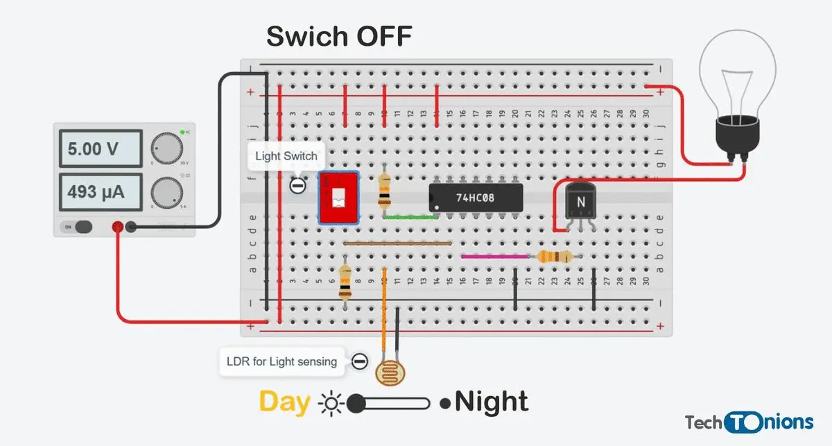
Therefore there are four possible cases-
- Daytime and input switch is OFF, and the output bulb is also OFF.
- Daytime and input switch is ON, and the output bulb is also OFF. (due to AND logic)
- Nighttime and input switch is OFF, and the output bulb is also OFF.
- Nighttime and input switch is ON, and the output bulb is ON.
To Simulate above code click open simulator button given below
It’s small automation based on light-sensing and digital logic AND gate operation, yet it can save lots of electricity.
You can build a similar project with one input from LDR and another input from the PIR sensor to the AND gate. These can be used as parking lights. Whenever car motion is detected, and there is less light in the parking area, it will turn on the Lights for a while and back OFF lights automatically when no motion is detected.
Like this, you can explore many AND gate applications around us in day-to-day life.
Maybe there are not using the same technique that we discussed, but this tutorial’s main concern was to teach how AND gate can be utilized in different applications.
Conclusion
Digital electronics is fun to learn, and we can do many things with digital logic AND gates. We need to find an application that matches the Truth table of AND gates.
If you like our content, then consider supporting us by subscribing to the weekly newsletter.